However, there is also a notable exception. Although semiconductor materials are also transparent in the infrared band, reliable welding between semiconductor materials cannot be achieved by using standard laser welding process.
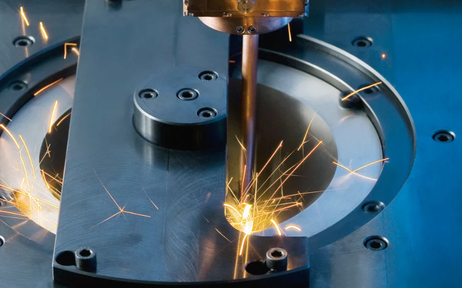
It is believed that this long-standing problem is due to the strong propagation nonlinearity in narrow bandgap materials, when the laser beam is focused below the material surface. It will cause defocus and form plasma before focusing (pre-focal plasmaformation)。 When the ultrafast infrared laser is focused inside the semiconductor, these phenomena generally prevent the effective energy deposition at the focal spot. This hinders any type of material modification, therefore, it also hinders the melting and subsequent re-curing at the interface of the welded parts.
In order to solve this problem, recent work has proposed a complex compensation program based on pulse sequence, focusing strategy or using longer pulse to reduce nonlinearity. The last method is to use a longer pulse to reduce the transmission nonlinearity, and can use picosecond pulse to demonstrate the coarse and fast laser “silicon metal” welding. The bottom material is metal. Metal can improve energy absorption; However, this method is still unable to realize semiconductor welding.
This is due to another important physical limiting factor, the binding defect between high refractive index semiconductor materials (the binding is not tight enough), which will lead to the gas source at the interface between the upper and lower materials. This air gland will act as a resonant optical cavity, driving energy density away from the interface.
Laser welding of silicon-silicon
Based on this important new discovery, researchers adopted a process configuration to avoid these two restrictions and realized the experimental demonstration of “silicon silicon” laser welding for the first time.
Using nanosecond pulse instead of ultrashort pulse, such as picosecond or femtosecond, to reduce transmission nonlinearity.On the other hand, let the two semiconductor workpieces to be welded in the closest optical contact state of F to avoid any gap at the interface. In this way, the “silicon silicon” laser welding was successfully demonstrated, and a high bonding strength of 30MPa was obtained.
Interestingly. The “silicon silicon” welding strength demonstrated has been better than the “silicon and metal” welding strength demonstrated for the first time, and is similar to the typical value obtained by the advanced molecular wafer bonding method.
Welding of different semiconductor materials
After the above successful experimental demonstration. The researchers also extended this method to gallium stellate (GaAs). The results show that this method can not only weld other semiconductor materials, but also weld different semiconductor materials. In these cases, the welding performance achieved by this method is also very high, and the average welding strength obtained by all tests is about 15Mpa.
Compared with other technologies applicable to the connection of semiconductor materials (such as molecular wafer bonding), the laser welding solution has unique advantages: it can weld complex semiconductor workpiece and a variety of semiconductor materials, which is difficult to do with other methods.
Because the laser beam can be guided accurately, it is not necessary to process the whole wafer or large wafer before welding. By selectively irradiating the area to be welded, small workpieces with complex shapes can easily achieve high-precision welding.
This opens the door for new manufacturing practices in electronics, mid-infrared photonics and micro-electromechanical systems (MEMS). In addition, this flexible assembly process also brings potential for the development of hybrid chips, for example, electronic and microfluidic systems jointly designed for sustainable cooling solutions in demanding semiconductor technologies.
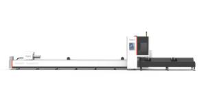
The effective welding between semiconductor materials is realized by using the compact nanosecond fiber laser source in the infrared band. This breakthrough is expected to further expand the application range of laser welding.
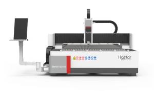
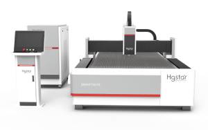
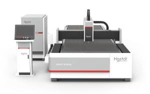
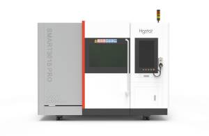
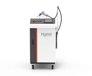
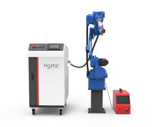
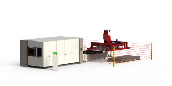
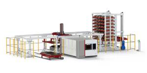
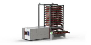
About HGSTAR: HGSTAR is is a sub-brand of HGTECH.HGTECH the pioneer and leader of laser industrial application in China, and the authoritative provider of global laser processing solutions. We have comprehensively arranged laser intelligent machine, measurement and automation production lines, and smart factory construction to provide overall solutions for intelligent manufacturing.