PCB (printed circuit board) is widely used in the automotive industry, and can be found in automotive electronics, sensors, lighting systems, and many other automotive applications. In applications with high safety requirements, PCBs must meet high quality standards, so we must be careful with every detail of the PCB production process.
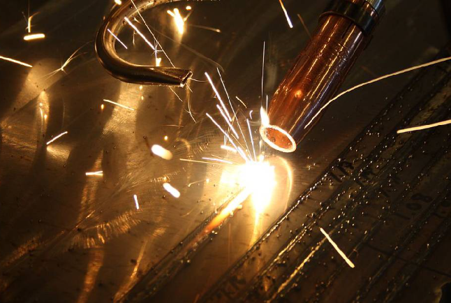
First of all, using lasers to cut PCBs is different from using machines such as milling or stamping. Laser cutting does not leave dust on the PCB, so it does not affect later use. Moreover, the mechanical and thermal stresses of components introduced by lasers are small enough to be negligible, and the cutting process is quite mild.
Secondly, laser technology can meet the requirements for cleanliness. It is possible to produce PCB with high cleanliness and high quality by non carbonization and non discoloration treatment of the substrate. In addition, in order to prevent faults during the cutting process, phase loss design is also made in the product to prevent them. Therefore, users can obtain extremely high yield in production.
In fact, by adjusting parameters, people can use the same laser cutting equipments to process various materials, such as standard applications such as FR4 or ceramic products, insulated metal substrates (IMS), and system level packaging (SIP). This flexibility enables PCB applications in various scenarios, such as engine cooling or heating systems, chassis sensors, and so on.
In PCB design, there are no restrictions on contour, radius, label, or other aspects. Through full circumference cutting, the PCB can be placed directly on the table, greatly improving the efficiency of space use. Compared to mechanical cutting technology, using laser to cut PCB can save more than 30% of material. This not only helps to reduce the cost of producing specific purpose PCBs, but also helps to build a friendly ecological environment.
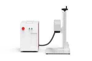
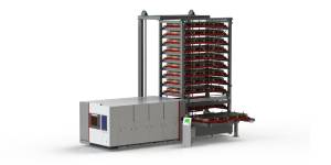
Laser systems can easily be combined with existing manufacturing execution systems (MES). The advanced laser system ensures the stability of the operation process, while the automatic characteristics of the system also simplify the operation process. Due to the higher power of the integrated laser source, current laser machines can completely compete with mechanical systems in cutting speed. Moreover, the operating cost of the laser system is low, and there are no worn parts (such as milling heads). Therefore, the cost of replacing parts and the resulting downtime can be avoided.
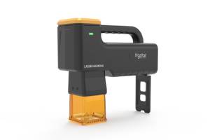
The application field of laser is very wide, in addition to being used for substrate cutting, it can also be used for welding, drilling, or ablation of individual material layers. It is also widely used in the cutting of solar silicon cells.
The traditional silicon wafer cutting method is mechanical cutting, which is slow in speed, poor in section flatness, numerous fragments, and not environmentally friendly. Silicon is a brittle material, and mechanical cutting can easily cause cracks at the edges, causing damage to the constituent layers of the elastic strain region, dislocation network region, and broken crystal region on the surface of silicon, and even potentially causing hidden cracks that affect electrical parameters. Laser cutting technology has the advantages of non-contact, no mechanical stress, small cutting seam width, smooth and smooth cross-section, high accuracy, fast speed, and stable performance; It does not damage the structure of silicon wafers, and its electrical parameters are superior to traditional mechanical cutting methods. It can be applied to line cutting of large area battery wafers, achieving precise control of cutting accuracy and thickness, further reducing cutting debris, and improving battery utilization.
The interaction time between the laser and the processed material can be controlled, thereby controlling the heat input to the workpiece, making the range of process debugging for processing different materials more extensive.
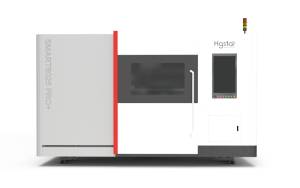
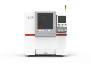
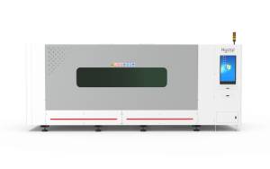
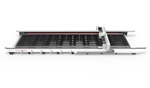
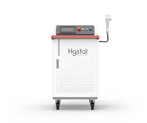
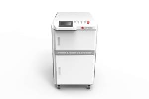
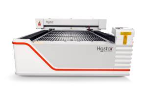
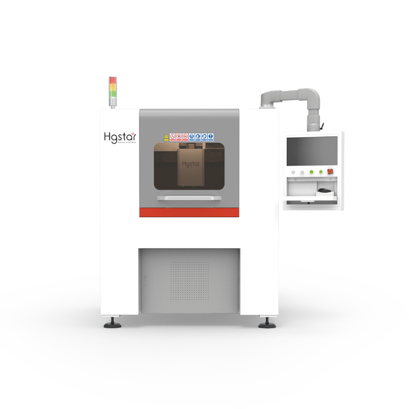
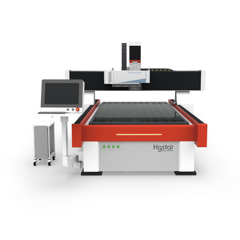
About HGSTAR: HGSTAR is is a sub-brand of HGTECH.HGTECH the pioneer and leader of laser industrial application in China, and the authoritative provider of global laser processing solutions. We have comprehensively arranged laser intelligent machine, measurement and automation production lines, and smart factory construction to provide overall solutions for intelligent manufacturing.