PCB and FPC industries are rapidly developing, with huge market growth
PCB, abbreviated as Printed Circuit Board, is one of the important components in the electronic industry and is used in almost all electronic products. Its main function is to achieve electrical interconnection between various components. PCB is composed of an insulated base plate, connecting wires, and a solder pad for assembling and welding electronic components, which has a dual function of conducting wires and insulating base plates. Its manufacturing quality can directly affect the reliability of electronic products, making it the fundamental industry in today’s electronic information product manufacturing and the industry with the largest output value in the global electronic component segmentation industry.
The application market of PCB is very extensive, including consumer electronics, automotive electronics, communication, medical, military, aerospace, etc. At present, consumer electronics and automotive electronics are developing rapidly and have become the main areas of PCB application. For a long time, the global PCB output value has been mainly concentrated in North America, Europe, and Japan. After 2000, the focus of the PCB industry began to shift to the Asian region, with the Chinese market being the most prominent. In 2009, the output value of Chinese Mainland’s PCB industry accounted for about 1/3 of the world, and by 2017 it had reached 50.5%, accounting for half of the global PCB output value.
Affected by trade frictions, declining terminal demand, and exchange rate depreciation, the global PCB output value has slightly decreased. However, the Chinese market has benefited from the rapid development of industries such as 5G, big data, cloud computing, artificial intelligence, and the Internet of Things, becoming the only region to grow in 2019. According to data, the size of the Chinese PCB market in 2019 was approximately 32.9 billion US dollars, accounting for 53.7% of the global market.
In the PCB application of consumer electronics, FPC has the fastest development speed and its proportion in the PCB market is constantly increasing. FPC is the abbreviation of Flexible Printed Circuit. It is a highly reliable and excellent flexible printed circuit board made of polyimide (PI, also known as PI covering film in industry) or polyester film as the substrate. It has the characteristics of high wiring density, light weight, thin thickness and good bending performance. In the current trend of intelligent and lightweight mobile electronic products, FPC is widely used with advantages such as high density, light weight, thin thickness, bending resistance, flexible structure, and high temperature resistance, and has become the only solution to meet the miniaturization and mobility requirements of electronic products.
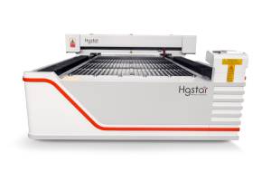
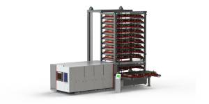
The rapidly developing PCB market has cultivated a huge derivative market. With the development of laser technology, laser processing has gradually replaced traditional die-cutting processes and become an important part of the PCB industry chain. Therefore, in the context of a slowdown in the overall growth rate of the laser market, PCB related businesses can still maintain high growth.
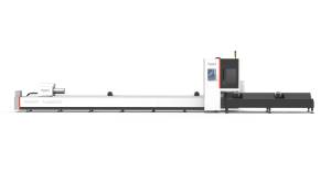
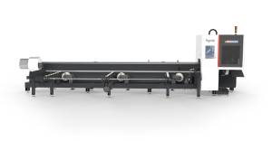
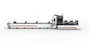
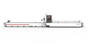
Advantages of laser in PCB and FPC processing
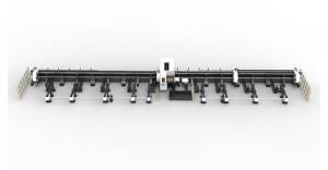
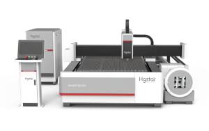
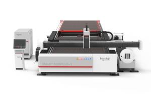
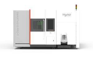
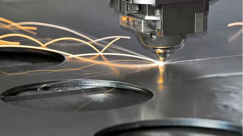
The application of laser on PCB mainly includes cutting, drilling, marking, etc., with cutting being the main focus. Compared with traditional die-cutting processes, laser cutting belongs to non-contact processing and does not require expensive molds, greatly reducing production costs; In addition, traditional processes are difficult to solve a series of problems such as burrs, dust, stress, and inability to process curves on the edges. However, the laser spot after focusing is only about ten micrometers, which can meet the processing needs of high-precision cutting and drilling, and solve a series of problems left over from traditional processes. This advantage caters to the trend of precision circuit design and is an ideal tool for PCB, FPC, and PI film cutting.
In fact, the application of PCB laser cutting technology in the PCB industry started early, but the early use of CO2 laser cutting had a significant thermal impact and low efficiency, and has not been able to achieve good development. It has only been applied in some special fields such as scientific research and military industry. With the development of laser technology, more and more light sources can be applied in the PCB industry, which has also found a breakthrough for the industrial application of laser cutting PCBs.
In principle, pulsed laser cutting materials can be divided into two situations: one is the photochemistry principle, which uses laser single photon energy to reach or exceed the chemical bond energy of materials, and breaks some chemical bond of materials to achieve cutting; The other is the principle of photophysics. When the single photon energy of the laser is lower than the chemical bond energy of the material, it depends on the very high energy density at the focus spot to exceed the gasification threshold of the material, so that the material can be instantly gasified and the material can be cut. But in reality, when using ultraviolet laser to cut FPC or PI films, the principles of photochemical and photophysical cutting coexist.
China’s PCB industry has benefited from the rapid development of emerging industries such as 5G and big data, and the emergence of new industries and technologies has also put forward higher requirements for the FPC and PI film cutting industries. In order to achieve less carbonization and faster efficiency, laser companies are also constantly undergoing technological innovation, exploring higher frequencies, narrower pulse widths, and higher power.
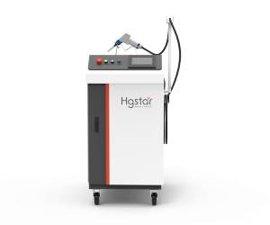
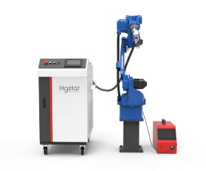
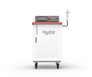
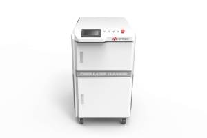
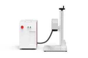
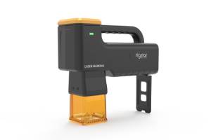
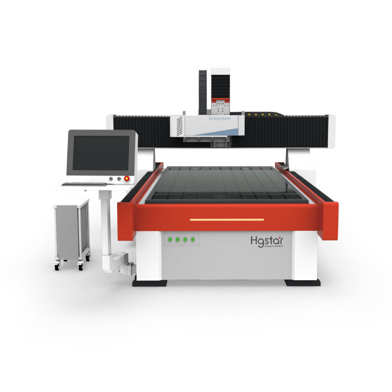
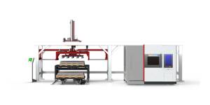
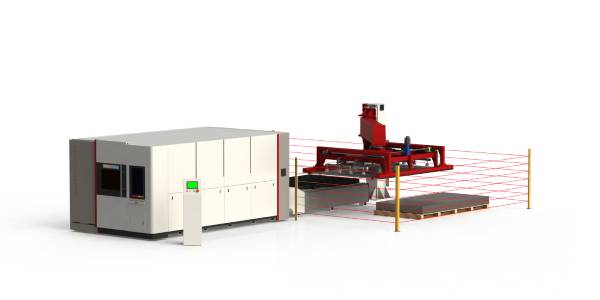
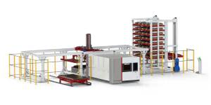
About HGSTAR: HGSTAR is is a sub-brand of HGTECH.HGTECH the pioneer and leader of laser industrial application in China, and the authoritative provider of global laser processing solutions. We have comprehensively arranged laser intelligent machine, measurement and automation production lines, and smart factory construction to provide overall solutions for intelligent manufacturing.